JNTE 2022 > Présentations plénières et invitées
Présentation plénière

3D LASER MICRO- AND NANOPRINTING
Keywords : laser printing, two-photon absorption, two-step absorption, light-sheet 3D printing, 3D metamaterials, printed electronics, 4D printing
Following a brief introduction into 3D laser printing on the micrometer and nanometer scale based on two-photon absorption [1,2], I will emphasize recent progress of my group in this field.
This includes replacing two-photon absorption by one-color two-step absorption, allowing to use compact and inexpensive continuous-wave lasers rather than femtosecond laser systems [3]. Using two-color two-step absorption combined with the idea of light-sheet laser printing [1,4], we have more recently achieved print rates approaching 107 voxels/s.
Aligning the director of liquid-crystal elastomers during the 3D laser printing process yields 3D micro-architectures that can be actuated by light from an LED [5].
Finally, I briefly discuss recent unpublished [6] progress in regard to laser printing of functional microelectronic devices such as diodes, memristors, and transistors. Here, introducing laser-induced photothermal synthesis of inorganic semiconductors such as ZnO has been crucial.
References
[1] V. Hahn et al., “3D Laser Nanoprinting,” Opt. Photonics News 30, 28 (2019).
[2] V. Hahn et al., “Rapid assembly of small materials building blocks (voxels) into large functional 3D metamaterials,” Adv. Funct. Mater. 30, 1907795 (2020).
[3] V. Hahn et al., “Two-step absorption instead of two-photon absorption in 3D nanoprinting,” Nature Photon. 15, 932 (2021).
[4] V. Hahn et al., “Light-sheet three-dimensional microprinting via two-colour two-step absorption,” Nature Photon., in press (Oct. 2022).
[5] A. Münchinger et al., “3D Optomechanical Metamaterials,” Mater. Today, in press (2022); https://doi.org/10.1016/j.mattod.2022.08.020.
[6] L. Yang et al., “Laser printed microelectronics,” submitted (2022).
Short biography
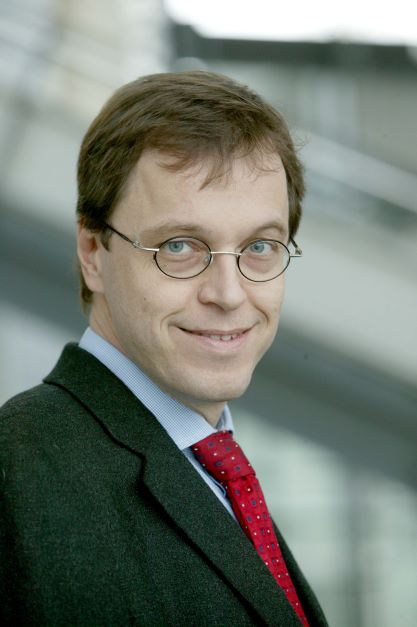
After completing his Diplom and PhD in physics at Johann Wolfgang Goethe-Universität Frankfurt (Germany) in 1986 and 1987, respectively, Martin Wegener spent two years as a postdoc at AT&T Bell Laboratories in Holmdel (U.S.A.). From 1990-1995 he was professor (C3) at Universität Dortmund (Germany), since 1995 he is professor (C4, later W3) at Institute of Applied Physics of Karlsruhe Institute of Technology (KIT). Since 2001 he has a joint appointment as department head at Institute of Nanotechnology (INT) of KIT, from 2016-2022 he was one of three directors at INT. From 2001-2014 he was the coordinator of the DFG-Center for Functional Nanostructures (CFN) at KIT. Since 2018 he is spokesperson of the Cluster of Excellence 3D Matter Made to Order. His research interests comprise ultrafast optics, (extreme) nonlinear optics, optical laser lithography, photonic crystals, optical, mechanical, electronic, and thermodynamic metamaterials, as well as transformation physics. This research has led to various awards and honors, among which are the Alfried Krupp von Bohlen und Halbach Research Award 1993, the Baden-Württemberg Teaching Award 1998, the DFG Gottfried Wilhelm Leibniz Award 2000, the European Union René Descartes Prize 2005, the Baden-Württemberg Research Award 2005, the Carl Zeiss Research Award 2006, the Hector Research Award 2008, the SPIE Prism Award 2014 for the start-up company Nanoscribe GmbH, the Stifterverband Science Award – Erwin-Schrödinger Prize 2016, and the Technology Transfer Prize of the German Physical Society (DPG) 2018. In 2014, 2015, 2016, 2017, 2018, 2020, and 2021 Clarivate Analytics listed him as “Highly Cited Researcher” (top 1%). He is Member of Leopoldina, the German Academy of Sciences (since 2006), Member of acatech, the National Academy of Science and Engineering (since 2019), Member of the Hector Fellow Academy (since 2013, President from 2016-2022), Fellow of the Max Planck School of Photonics (since 2019), Fellow of the Optical Society of America (since 2008), and Honorary Professor at Huazhong University of Science & Technology, Wuhan, China (since 2014).
Présentations invitées
| Intervenants | Titre | Date |
|
Isabelle Sagnes - INSIS CNRS |
Les programmes nationaux autour des nanotechnologies au CNRS |
Wed. 09h00-9h30 |
|
Martin Wegener - KIT |
Wed. 09h30-10h15 |
|
|
Remi Dreyfus - ESPCI/LN2 Sherbrooke |
Wed. 10h15-10h45 |
|
|
Nicolas Triomphe - CBS Montpellier |
Self-assembly of DNA origamis for nanolithographic applications |
Wed. 11h00-11h30 |
|
Gwenaël Bécan - MISTIC Technologies |
Wed. 14h00-14h30 |
|
|
Jean-Marc Linares - ISM Marseille |
Wed. 14h30-15h00 |
|
|
Caterina Tomba - INL Lyon |
Wed. 16h00-16h30 |
|
|
Karla PEREZ TORALLA - CEA Saclay, Laboratoire d'études et de recherches en immunoanalyse |
Wed. 16h30-17h00 |
|
|
M. de Labachelerie, B. Lecha - FEMTO-ST, IEMN |
Réseaux plateformes / EuroNanoLab et Renatech-projets |
Thur. 08h30-09h00 |
|
Florent Doutre - FEMTO-ST/LAAS/INPHYNI |
Thur. 09h00-09h30 |
|
|
Karim Ouaras - LPCIM Palaiseau |
Growth of crystalline III-V thin films using low-temperature plasma |
Thur. 10h30-11h00 |
|
Vincent Rat - IRCER Limoges |
Dépôts de couches céramiques par projection thermique: procédés et applications |
Thur. 11h00-11h30 |
|
Paolo Bondavali -TRT |
Matériaux 1D-2D par la méthode de dépôt LEGO |
Thur. 12h00-12h30 |
|
Julien Granier - Manutech-usd |
Thur. 14h00-14h30 |
|
|
Céline Chevalier - INL - Réseau JNIL |
Thur. 14h30-15h00 |
|
|
Xin Guan - TUE Holland |
In-situ device fabrication in Molecular Beam Epitaxy Cluster |
Thur. 16h00-16h30 |
|
Philippe Lombard - Ampère Lyon |
The potential of 3D Plastronics: from packaging to ecofriendly innovative systems |
Fri. 08h30-09h00 |
|
Maximilien Billet - Ghent University |
Fri. 09h00-09h30 |
|
|
Yoshio MITA - Univ. of Tokyo, LIMMS |
Flexiboard: CMOS-MEMS chiplet integration with soft materials towards autonomous programmable matter |
Fri. 10h30-11h00 |
|
Sébastien Plissard - LAAS Toulouse |
Nanofabrication of topological insulators |
Fri. 11h00-11h30 |
|
Vincent Astié - Annealsys |
2D materials by chemical vapor deposition: from coupons to large area depositions |
Fri. 12h00-12h30 |


